Topview Simulator R8C/Tiny Devices.
Introduction.
SANGO - R8C/Tiny System Simulator gives an excellent simulation environment for the industryĺs most popular 16-bit microcontroller family,
R8C/Tiny. It gives all required facilities to enable the system designers to start projects right from the scratch and finish them with ease and confidence.

SANGO is the total solution giving many state of art features meeting the needs of the designers possessing different levels of expertise. If you are a beginner, then you can easily learn about R8C/Tiny based embedded solutions without any hardware. If you are an experienced designer, you may find most of the required facilities built in the simulator enabling you to complete your next project without waiting for the target hardware.
Device Selection.
Devices in the groups R8C/11, R8C/13, R8C/1A, R8C/1B, R8C/24 and R8C/25 of R8C/Tiny family are supported.
Program Editing.
Powerful editing features for generating your programs and the facility to call an external Assembler to process input programs.
ClearView.
ClearView facility gives all the internal architectural details in multiple windows. Information about the Program, Memory, Registers, SFRs are clearly presented in many windows to make you understand the program flow very easily.
Program Execution.
A variety of program execution options including Single Stroke full speed execution, SingleStep, StepOver and BreakPoint execution modes give you total control over the target program.
ClearView updates all the windows with the correct and latest data and it is a convenient help during your debugging operations.
You may find this Simulator simplifies the most difficult operation of the program development, debugging, into a very simple and interesting task.
Simulation Facilities.
Powerful simulation facilities are incorporated to complete your next embedded solution:
- CPU configuration for the application.
- Facility to develop the programs and also verify them.
- On-chip clock structure, interrupt facilities.
- All the on-chip peripherals including ports, timer/counters, communication facilities.
- Facilities are available to use all the features of the selected micons without any physical hardware.
- Also plenty of external embedded modules are simulated for the application.
- Range of Plain Point LEDs and Seven Segment LED options.
- LCD modules in many configurations.
- Momentary ON keys.
- A variety of keypads upto 4 X 8 key matrix.
- Toggle switches.
- All modes of onchip serial port communication facility.
- IIC components including RTC, EEPROMs.
- SPI Bus based EEPROM devices.
Code Generation Facilities.
Powerful and versatile Code Generating facility enables you to generate the exact and compact code for many possible application oriented interfacing options.
You can simply define your exact needs and get the target code at a press of button at anywhere in your program flow. The code gets embedded into your application program automatically.
You are assured of trouble free working of final code in the real time.
- All on-chip peripherals including CPU clock selection.
- Interfacing IIC/SPI Bus devices.
- Range of keypads.
- Many LED/LCD interfacing possibilities.
Device Selection and Clock Setting.

Select the device group from the list.
 Select the device group from the list. Select the device group from the list.
 Select a particular device form the list of devices. Select a particular device form the list of devices.
 The features of the selected device will be displayed here. The features of the selected device will be displayed here.
 Check the check box to connect external clock to system. Check the check box to connect external clock to system.
 Enter the frequency of the external clock in Hz. Enter the frequency of the external clock in Hz.
 Some of the devices have facility to connect a sub clock with frequency of 32.768 KHz. If the check box is enabled, the subclock will be connected to the controller. Some of the devices have facility to connect a sub clock with frequency of 32.768 KHz. If the check box is enabled, the subclock will be connected to the controller.
 Click OK button to start the simulator with the environment meant for the selected device. Click OK button to start the simulator with the environment meant for the selected device.
ClearView Window Structure.
This is an optimized arrangement where windows are strategically placed in the display. Display area of the monitor is divided into five windows. Windows meant for Program, Register, RAM Area, Code Area, and SFR are placed in the ClearView. Size and position of the windows canĺt be changed. Scrolling facility is available wherever it is required.
This ClearView gives a complete picture on the internal architecture in a single screen while debugging the program code.

I/O Simulation Window

Displays the input levels of each port line and facility is available to set Ĺ0ĺ or Ĺ1ĺ level to the input line.
Indicates the output levels of all port lines.
To simulate ADC , a third option ĹAnalogĺ to the respective port lines is provided. If this option is selected to a particular port line, a variable analog input source is enabled for that line along with the analog reference source.
To simulate interrupts and timers with external clock, a fourth option called ĹPulseĺ is provided for the respective lines. A button is available to generate pulses to the timer or interrupt lines.
I/O window comes with all the ports of I/O lines with facility to simulate timers/counters at the respective I/O pins. Interrupt conditions can be simulated. Facility to test ADC is also available in this window.

A variable source is connected to the port line, if ĹAnalogĺ option of that line enabled. A slider control is provided for this purpose. Using this slider, the voltage level to the selected port line can be varied. The simulated voltage gets displayed. Maximum voltage input is 5V.
A variable source is connected to the Vref of the ADC using another slider. Maximum voltage input is 5V.
CPU Status Window.

Gives the details of the external main clock, its status and its frequency. The frequency can also be edited here for the target application.
Displays the status of the high speed on-chip oscillator: The frequency of the high speed oscillator and its division ratio.
Displays the status of the low speed on-chip oscillator along with its frequency of oscillation.
Gives the details of the external sub clock, its status and its frequency.
Gives the details of selected CPU clock (either external main clock or on-chip oscillators or external sub clock)
Gives the details of the voltage detection circuit 0.
Gives the details of the voltage detection circuit 1.
 Gives the details of the voltage detection circuit 2. Gives the details of the voltage detection circuit 2.
 The CPU voltage can be increased or decreased using this slider. By altering the CPU voltage, the voltage detection operation can be similated and examined when using this window. The CPU voltage can be increased or decreased using this slider. By altering the CPU voltage, the voltage detection operation can be similated and examined when using this window.
 Gives details of the oscillation circuit, whether the circuit is oscillating or not and about the Oscillation Stop Detection Circuit. Gives details of the oscillation circuit, whether the circuit is oscillating or not and about the Oscillation Stop Detection Circuit.
 The details of watchdog timer, its status, underflow time and the timer count value are indicated. The details of watchdog timer, its status, underflow time and the timer count value are indicated.
The CPU Status window gives the details of the CPU clock frequency, on-chip oscillators, voltage detection circuits, watchdog timer, etc.
Simulated Host for Serial Port.

Host window acts as the host to the serial port UART0, UART1 and SSU.
Displays the serially received data.
Transmits the data serially with the defined baud rate and format.
Select the channel UART0 or UART1 or SSU.
Select the mode Synchronous or Asynchronous.
Select the 9th bit data for multiprocessor
communication.
Choose the format ľ LSB first / MSB first.
Choose the baud rate for transmission and reception.
Select the no of bits for Asynchronous mode 7 bits / 8 bits / 9 bits.
Select the parity type for Asynchronous mode ľ no parity / even / odd
Choose the stop bits for Asynchronous mode.
Choose the Clock polarity for Synchronous mode.
 Choose the display format for both the buffers. Choose the display format for both the buffers.
 Host Setting ľ Transfer data from file or the entered byte in the window. Host Setting ľ Transfer data from file or the entered byte in the window.
 Enter data for transfer. Enter data for transfer.
 Click this button to clear both the buffers. Click this button to clear both the buffers.
 This setting applies for Synchronous mode and SSU mode. Select the host to simulate a master or a slave. This setting applies for Synchronous mode and SSU mode. Select the host to simulate a master or a slave.
 Select the file, to transfer from the host. The file transfer details are displayed. Select the file, to transfer from the host. The file transfer details are displayed.
On-chip Serial Port Simulation.

This window simulates both the channels of the
serial port.
Receiver buffer for channel 0.
Transmit buffer for channel 0.
Receiver buffer for channel 1.
Transmit buffer for channel 0
Select the display format for all buffers.
Clear both the buffers for channel 0.
Simulated Host for the SSU.

This window is the simulated host for the on-chip SSU.
Enable the Simulated Host for the IIC module.
Select the mode: Maser or Slave.
Select the Slave address.
Enter the data to be sent.
Select the clock speed.
Click this button to start the operation.
Click this button to Clear the summary window.
Select the no of bits for Asynchronous mode 7 bits / 8 bits / 9 bits.
The available operations for the selected mode Master is listed here.
Choose the stop bits for Asynchronous mode.
Displays the commands in the sequence selected by user.
The completed operations are listed here.
LCD Module Configuration for Simulation.

Check the checkbox to enable the LCD module.
Select the LCD type.
Select the interface type as parallel.
Choose the data bus width from two options: 8bits or 4bits.
Switch on back light for LCD.
Displays the control and data lines of the LCD.
Allocate port lines for control and data lines of the LCD.
Displays the details of the port lines
allotted for the LCD module.
Press this button to disconnect all the port lines from the LCD module.
Fixed level like Ĺ0ĺ or Ĺ1ĺ can be selected using this option to reduce the port line usage.
BreakPoint Setting.

Displays the source for the breakpoint setting.
Displays the list of registers available for the selected source.
Displays the details of the selected BreakPoint.
Code Generation.
Code generation facility is available for all on-chip peripherals and external peripherals. Place the cursor at the point on the opened text file in the simulator. From the Code generation menu any module is selected and after proper settings code is generated and gets pasted at the cursor point.
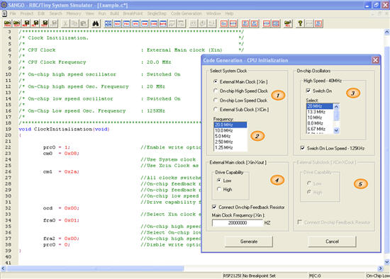
Code for CPU Initialization.
Select the system clock from the options available.
The selected clock and its divisions available are displayed in the list box. Choose the system frequency from the list.
Options are available for the on-chip oscillators. Select them if code is required.
Options for external main clock.
Options for external sub clock.
Click generate button to generate the code.
Code Generation for Two Lines by 16 Characters LCD Interface.

Select the required routines.
Select the LCD type and
initialization setting.
The control lines and
selected port lines are
displayed as summary.
Select the port lines for the
control lines. Error checking
also included. (ie. A single
port line cannot be selected
for two or more control lines)
Code Generation for Internal Peripheral - Timer RA.
Code is generated for all the available modes of the Timer RA. For example the ĹPulse output modeö is discussed here.

Mode selection. Available modes are listed here.
Enter the prescalar and counter values. The frequency of the waveform gets displayed in a static box at the bottom. Adjust the counter values and set the required frequency.
Set the priority level for the timer RA overflow interrupt.
Select the clock source for timer.
Select the sampling clock for digital filter if required.
Select the port line for TRAIO output.
Select the output level for TRAIO pin.
Select the oscillator for fOCO clock.
Choose the clock divider
Click the generate button to generate the code.
Project Management.

SANGO gives you facility to develop your programs right from the scratch. SANGOĺs built-in Text Editor takes care of program entry operations. You can also downl9oad any input program from the disk.
Program development starts by creating a new project. The project window gives the details of the files used in the project.
The editor window displays the contents of the ĹCĺ files.
The project files can be compiled using the ĹCĺ Compiler for R8C/Tiny. The compiler output is captured and displayed in the Output window. Use ĹDowloadĺ option to download the mot file in to the simulator for testing.
Example 1 - Study of On-chip ADC with 8 Numbers of Point LEDs.

In this example the on-chip ADC is read and the digital data from ADC is displayed on eight numbers of point LEDs. The ADC is configured in 8 bit, one shot mode. The variable analog voltage can be given to the selected ADC input through the slider provided in the I/O window.
For study purpose, channel 7 of ADC is used and the point LEDs are connected to the port line P1_0 to P1_7.
In the program, the start conversion signal is given, and the converted digital data is read from ADC after getting the end of conversion signal. The read digital data is send to the port 1. This process is repeated continuously.
Example 2 - Two Lines by 16 Characters LCD Interface.

This example deals with the interfacing of a two lines by 16 characters LCD module with micon in 4bit bus mode. Port lines P2_1 to P2_3 are connected to the control lines RS, R/W and E. The port lines P2_4 to P2_5 are used to send the data to LCD module.
In the program, the LCD module is first initialized in 2 lines, 4 bit bus mode. Then a 2 line message is displayed on LCD as shown in the figure.
Example 3 - Serial Port.

This study example gives a picture of the on-chip serial port and the simulated host serial port in asynchronous mode.
The UART0 of R8C/Tiny micon is used in this study at 9600 baud rate. In the program, the UART0 is initialized at 9600 baud and a message ôTestingůö is sent to the host.
The host will receive the message and displayed the same on the screen. Data transmitted and received for both on-chip UART and the host are displayed on screen as shown.
There is an option to select the display format as either ASCII or Hex.
Project - Programmable Timer.
This is an R8C/Tiny based useful timer meant for controlling a relay/solenoid as per timing schedule. It can be used in many applications where it is required to switch On/Off lights, motors and etc. at the fixed predefined timings.
The hardware is very simple. The R8C/Tiny micon controls every thing. There is an IIC RTC available to keep track of the current time. The LCM with 2 line X 16 size display combines with the keyboard to give the required interacting facility.
Download Topview Simulator.
To download Topview Simulator
for the R8C/Tiny
Microcontrollers free of cost, Click here!
|